The Kill-a-Watt: Not all versions are created equal :)
There are several different versions of the “Kill-a-Watt” power-measurement appliance on the market. They all have essentially exactly the same electronic design, but they’re a little bit different in terms of the PCB layout, packaging and component package choices. This device is one of the most often hacked and modified devices of its kind on the market, so it’s good to try and get a little bit of an understanding of what it has inside.
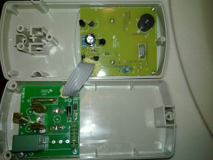
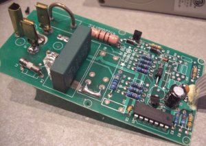
Here’s one version. It contains the transformerless power supply (the large capacitor, large resistor, zener diode and rectifier diode) as well as the current measurement shunt on their own PCB; the PCB that also holds the mains plug and socket contacts.
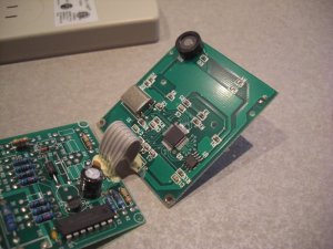
The 5V regulator, op-amps, microcontroller, EEPROM and LCD display are on a second, separate PCB. Here, the op-amp chip (a LM2902, which is equivalent to the very common LM324 quad op-amp) and the EEPROM (a pretty standard 8-pin I2C serial EEPROM) are both in surface-mount SOIC packages and they’re both mounted on the front side of the PCB, along with the main microcontroller IC (which is packaged in the cheap and nasty mass produced chip-on-board or COB technique, where a naked silicon die is mounted on the PCB, connected up with wire bonds and then covered in a blob of conformal epoxy) and the pads which connect to the conductive-rubber zebra connector which connects to the LCD display.
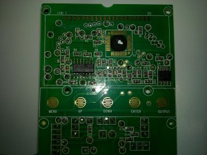
The six wires from the transformerless power supply board to the microcontroller board bring over the 240VAC active and neutral into the voltage-measurement op-amp (configured as a differential amplifier with significant attenuation), both sides of the current shunt resistor, into a differential amplifier, and the floating positive DC rail and the device’s DC ground from the transformerless power supply.
Of course, sampling the voltage waveform is very useful as it allows the true mains voltage to be measured, along with things like the power factor.
(Please remember that the Kill-a-watt uses a transformerless power supply, and you have to be extremely careful if you’re attempting any kind of interface to external electronics. It must be optically isolated, with an independent power supply on both sides of the optoisolators.
Basically, there is a 5V potential difference between the microcontroller’s Vdd and Vss rails, but there is *not* a potential difference of 5 volts between the microcontroller’s Vdd rail and mains earth – the 5V rail inside the kill-a-watt will in fact be at about 120VAC or 240VAC relative to mains earth. All the components inside are at the live AC mains potential relative to mains earth.
So if you just bring out a digital line – I2C or serial or whatever it is – from inside the Kill-a-Watt’s microcontroller and connect it to another external microcontroller with a conventional power supply, that external microcontroller will see 120 VAC on that line, relative to its own DC ground. Which is a Bad Thing.)
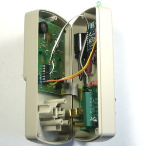
There’s also a slightly different variant, where the microcontroller, EEPROM and op-amp are all on the main board, and almost all of the components on the main board are surface mount, but the op-amp is replaced with a DIP through-hole package mounted on the back side (the non-copper side) of the board.
Here’s a photo of this version.
(Photo courtesy of Limor Fried, and used (pinched) in good faith. Please check out the great products available from Adafruit Industries :) )
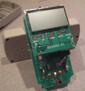
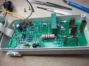
Now, here’s a different version. In this version, the mains input and output sockets, the transformerless power supply components, the voltage regulator components that generate the +5V and +6.2V rails, the op-amp chip and the components that are associated with the op-amp chip are all on a single board, and the LCD display, microcontroller and EEPROM are on a second board.
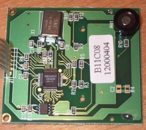
In this version, the LM2902 op-amp is in a through-hole DIP package, and through-hole resistors are used for the op-amp circuits. On the microcontroller board, the microcontroller is packaged in a standard package, which appears to be something like a 48-pin QFN. The chip’s label appears to be etched off, however. The EEPROM is still in a standard 8-pin SOIC package.
The six wires between the analog instrumentation board and the microcontroller board appear to be +5V, DC ground, two different analog outputs from the current measurement circuit into the microcontroller’s on-board ADC, the output from the voltage-measurement circuit into the microcontroller, and one more signal which I’m not completely sure about, but which I believe appears to be mains zero-crossing detection.
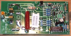
There appear to be a couple of slightly different batches of this model. One uses a X-class capacitor with a metallized polypropylene dielectric, in the moulded cuboid package, in the transformerless power supply circuit. A different variant uses a cheaper non-X-class red resin-dipped 630V polyester “greencap”.
(Images courtesy of Sparkfun, and used in good faith. Please support Nate and the team, they make nice things. :) )
Note the provision on the PCB for what appears to probably be a relay used to switch the mains load on and off, although it is not populated on the board on any of these units.
Note that the microcontroller (or ASIC) chip is labelled in the last picture, and it is branded by PRODIGIT out of China. It appears that all these devices are actually manufactured by PRODIGIT, and branded or badged under different names.
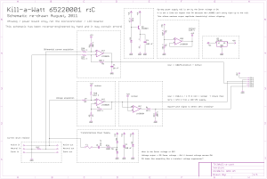
And finally, just for those of you who might be interested, here’s a schematic of the Kill-a-Watt. This is the schematic of the latter version described above, where the op-amp circuits are on the same board as the current shunt, the mains connectors and the transformerless power supply, with the microcontroller on a separate board.
This is only the schematic of the op-amp board, not the microcontroller board, and it is possible that this schematic might contain some bugs, and it might need some tweaks – check carefully! I hope it is helpful for you :)
About this entry
You’re currently reading “The Kill-a-Watt: Not all versions are created equal :),” an entry on Nullius in Verba
- Published:
- August 23, 2011 / 7:07 am
- Category:
- electronics, engineering, hardware hacking
- Tags:
2 Comments
Jump to comment form | comment rss [?] | trackback uri [?]